In today's wave of technology, microelectronics is like an invisible magician, quietly changing our lives. From smartphones to computer chips, from drones to self-driving cars, all this magic cannot be achieved without the participation of microelectronics. And behind microelectronics manufacturing, there is an indispensable and mysterious role - photolithography. So, what exactly is a photolithography machine? Today, let's walk into this core tool of microelectronics manufacturing, unveil its mysterious veil, and see how it injects life into our smart devices.
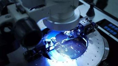
A photolithography machine is like the "plotter" of the semiconductor world. Its main job is to project tiny patterns of electronic circuits onto silicon wafers as accurately as we would draw on a wafer. The process is like using a special camera, but much more complicated than the ones we normally use. Photolithography uses ultraviolet light to "shoot" circuit patterns onto a silicon wafer through something called a mask, which makes it possible to create tiny electronic parts, such as miniature transistors and capacitors. In short, photolithography is the "master painter" of semiconductor manufacturing. Photolithography, as the name suggests, uses light-based imprinting technology. In the manufacture of microelectronic devices, photolithography is responsible for "printing" the designed circuit pattern on a special light-sensitive material. This process can be likened to our childhood game of "carving knife in the playdough lettering" game. Only, the photolithography machine "carving knife" uses precision optical systems and a high-precision motion platform, with very high speed and high precision in the "playdough" (light-sensitive materials) "carved" on the circuit pattern. "circuit pattern.
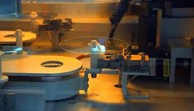
A photolithography machine operates like a giant projector. It uses a special light to illuminate a silicon wafer as if it were projecting an image on a canvas. However, it needs to go through very sophisticated optics and mechanical components to ensure that the final pattern is very fine and accurate, like a beautiful painting in the world of microelectronics. The process is very complex and requires high-precision engineering to ensure the accuracy and reliability of chip manufacturing. Photolithography machines are very versatile. They are a key tool in the semiconductor industry, helping to make our electronic devices such as smartphones and computer chips. These machines can create tiny electronic components, much like building miniature cities.
Apart from this, photolithographs also play a role in the manufacture of LCD and OLED screens. They help us to see clear images on our TVs, mobile phones and computer screens. Also, lithography is very useful in the medical field. It can help make biochips, which are used to research and diagnose diseases and even help develop new drugs. Photolithography plays an important role in different fields, making our lives easier and healthier.
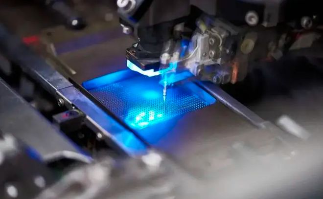
The importance of photolithography in the field of microelectronics cannot be underestimated. It is like the wizard of the microelectronics world, capable of creating countless tiny electronic spells. These magics include making computers faster, mobile phones smarter, batteries more durable, and many more amazing technologies. The constant innovation of photolithography is like a magic potion for our technological world, making everything more advanced and amazing.
Photolithography is like the magic paintbrush of microelectronics, creating minuscule but important electronic patterns on tiny silicon wafers. These patterns are the foundation of modern technology and they make our electronic devices smarter, faster and more powerful. By understanding photolithography, we can better understand why our computers, mobile phones and other electronics are so powerful.


